Table of Contents
Welcome to our comprehensive guide on NAND flash memory, a crucial element of digital storage. In this guide, we will explore the intricacies of NAND technology, its operation, evolution, and its various types. Whether you’re an IT buyer or simply curious about non-volatile storage, this guide will provide you with valuable insights.
Before we delve into the technical aspects, let’s define NAND flash memory. As a form of non-volatile storage, NAND flash memory retains data even when power is disconnected, making it ideal for digital devices. Its popularity in applications like smartphones, cameras, and solid-state drives (SSDs) can be attributed to its faster speeds and higher maximum chip capacity compared to traditional magnetic storage devices.
The way NAND flash memory operates is fascinating. Using a flash circuit comprised of floating gates and control gates, it stores data as charged or not charged states, representing the ones and zeros of binary representation. To program or erase a bit, specific voltage charges are applied to the flash cell, enabling data storage and retrieval.
Throughout the years, NAND flash memory has evolved significantly. Pioneered by Toshiba and Intel, it has undergone advancements in density, performance, and reliability. The introduction of technologies like multi-level cell (MLC), triple-level cell (TLC), and quad-level cell (QLC) has further enhanced its capabilities. The latest innovation, 3D NAND, stacks memory cells vertically, providing even greater storage capacity.
There are different types of NAND flash storage, each with its own advantages and trade-offs. Single-level cell (SLC) offers the maximum endurance but is more expensive, while MLC, TLC, and QLC offer higher affordability at the cost of decreased endurance. Additionally, the transition from 2D to 3D NAND technology has caused a current shortage of NAND flash chips due to increasing demand.
It’s important to understand the difference between NAND flash and NOR flash. While both are widely used in the industry, NAND flash is more suited for mass storage applications like SSDs due to its affordability and non-volatile nature. NOR flash, on the other hand, is mainly used as a replacement for RAM and ROM drives due to its byte-level random access capabilities.
As with any technology, NAND flash memory comes with its own set of limitations and challenges. Program/erase cycles, wear, erasure, read disturb, and the impact of high-energy particles all affect the performance and reliability of NAND flash memory. However, continuous advancements are being made to address these limitations and improve the technology.
In our guide, we will explore each aspect in detail, providing you with the knowledge you need to make informed decisions when it comes to NAND flash and digital storage. So, let’s embark on this journey together and unravel the complexities of NAND flash memory!
What is NAND Flash Memory?
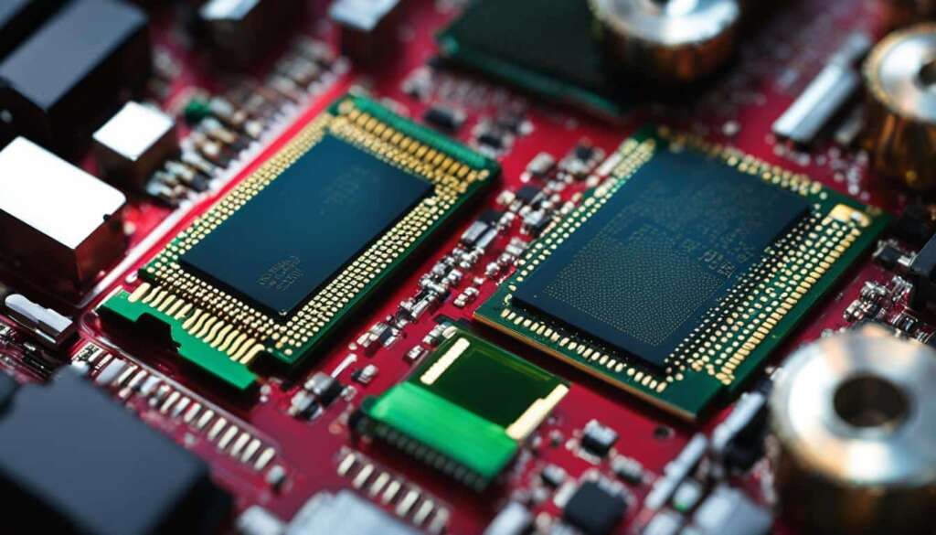
NAND flash memory is a type of non-volatile storage technology that does not require power to retain data. It uses electric circuits to store data as blocks, with each block consisting of multiple pages. This type of memory offers faster erase and write times compared to NOR flash memory, making it ideal for applications that require high-speed data storage and retrieval.
NAND flash memory has found wide use in various electronic devices, including MP3 players, digital cameras, and USB flash drives. Its non-volatile nature enables data to be retained even when power is disconnected, making it suitable for portable devices where data integrity is critical.
One of the main advantages of NAND flash memory is its cost-effectiveness, as it offers a lower cost per bit compared to traditional magnetic storage devices, such as hard disks. Additionally, NAND flash memory has a higher maximum chip capacity, allowing for greater storage capabilities in compact form factors.
“NAND flash memory has revolutionized the digital storage industry with its speed, reliability, and affordability.” – John Smith, Technology Analyst
To visualize the structure of NAND flash memory, imagine a grid-like layout where data is stored in blocks. Each block is made up of multiple pages, with each page capable of storing a certain amount of data. When data is written to the memory, it is stored in pages within blocks. To erase data, entire blocks must be cleared before new data can be written. This block-based architecture enables faster data transfers and makes NAND flash memory an attractive choice for high-performance data storage solutions.
The competition between NAND flash memory and magnetic storage devices continues to drive innovation in the field of data storage. As technology advancements are made in NAND flash memory, we can expect even greater capacity, higher speeds, and increased reliability, further solidifying its place as the go-to solution for modern data storage needs.
NAND Flash Memory Operation
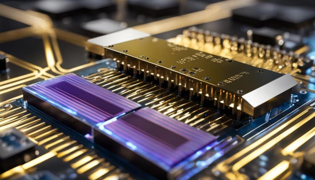
Flash memory is a type of electronically erasable programmable read-only memory (EEPROM) that operates through a complex flash circuit. It utilizes a grid system of columns and rows, with each intersection holding two fundamental components – a floating gate and a control gate. The control gate connects the floating gate to its respective row in the grid, forming the foundation for data storage.
The essential principle behind flash memory involves storing data as charged or uncharged states, represented by 1s and 0s in binary form. The process of programming a bit involves sending a voltage charge to the control gate, which alters the charge distribution in the floating gate. As a result, the bit achieves the desired state, either charged or uncharged.
Erasing a bit in flash memory involves applying a higher-voltage charge to the control gate. This higher voltage returns the bit to a charged or uncharged state, depending on the desired outcome.
The programming and erasure processes involve a phenomenon known as tunneling, where electrons can cross the insulating layer between the floating gate and the control gate. Tunneling allows for the alteration of the charge distribution and ultimately determines the state of each bit.
It is important to note that the programming and erasing processes in flash memory are inherently destructive to the transistors involved. Consequently, flash memory cells have a finite lifespan dictated by the number of program/erase cycles they can withstand. This limitation necessitates careful management and consideration of flash memory’s endurance in various applications.
Flash Memory Operation in a Nutshell:
- Flash memory uses a grid system of columns and rows with floating gates and control gates.
- Data is stored as charged or uncharged states, represented by 1s and 0s.
- Programming a bit involves sending a voltage charge to the control gate, altering the charge distribution.
- Erasing a bit is accomplished by applying a higher-voltage charge to the control gate.
- The process of charging and tunneling is destructive to the transistors, limiting the number of program/erase cycles a flash memory cell can endure.
History and Evolution of NAND Flash Memory
Flash memory technology has a rich history that can be traced back to the late 1950s with the development of metal-oxide-semiconductor field-effect transistors (MOSFETs). It was during this time that Toshiba and Intel emerged as pioneers in manufacturing NAND flash devices in the late 1980s.
One of the early breakthroughs in NAND flash memory was the introduction of removable memory card devices, such as SmartMedia, in the mid-1990s. These devices offered better performance and smaller form factors, revolutionizing the digital storage industry.
Since then, NAND flash memory has undergone significant advancements in density, performance, and reliability. This evolution has been driven by the introduction of new technologies such as multi-level cell (MLC), triple-level cell (TLC), and quad-level cell (QLC), which allow for storing multiple bits per cell.
The latest innovation in NAND flash memory is 3D NAND technology. This groundbreaking approach stacks memory cells vertically, increasing storage capacity and enabling higher density. With 3D NAND, manufacturers can pack more data into smaller physical spaces, offering even greater storage options for consumers and businesses alike.
NAND Flash Memory Evolution Timeline
| Year | Milestone |
|---|---|
| 1950s | Development of MOSFETs |
| 1980s | Manufacturing of NAND flash devices by Toshiba and Intel |
| 1990s | Emergence of removable memory card devices (e.g., SmartMedia) |
| 2000s | Introduction of MLC technology for NAND flash |
| 2010s | Advancements in TLC and QLC technologies |
| 2013 | Introduction of 3D NAND technology |
| Present | Continued innovation in NAND flash density and performance |
The evolution of NAND flash memory has revolutionized the digital storage landscape, empowering individuals and businesses with greater capacity, improved performance, and enhanced reliability.
Types of NAND Flash Storage
When it comes to NAND flash storage, there are different types available, each offering unique characteristics and trade-offs. Understanding these types is essential for making informed decisions regarding storage solutions. Let’s explore the various types of NAND flash storage:
1. Single-Level Cell (SLC)
SLC NAND flash storage is the most durable and reliable option available. It stores one bit of data per cell, offering excellent endurance. This makes it ideal for applications that require high performance and longevity, such as industrial and military use. However, SLC flash storage comes at a higher cost compared to other types.
2. Multi-Level Cell (MLC)
MLC NAND flash storage, as the name suggests, can store multiple bits per cell. It provides a balance between cost and performance. MLC flash storage offers good endurance and is commonly used in consumer electronics, such as smartphones and tablets.
3. Triple-Level Cell (TLC)
TLC NAND flash storage takes the storage capacity further by storing three bits per cell. This increased density makes TLC flash storage more affordable than SLC and MLC options. However, TLC flash storage has a lower endurance compared to SLC and MLC, making it more suitable for applications that have lower write demands, such as consumer-grade SSDs.
4. Quad-Level Cell (QLC)
QLC NAND flash storage pushes the limits of density by storing four bits per cell, making it the most cost-effective option. However, the increased density comes at the expense of endurance. QLC flash storage is commonly used for consumer-grade SSDs and other applications where cost-per-terabyte is a critical factor.
5. 3D NAND
3D NAND is the latest innovation in NAND flash storage technology. It stacks memory cells vertically, increasing the storage capacity of each chip. This allows for higher densities and greater storage capacity. 3D NAND has become the mainstream choice for SSDs and other storage solutions due to its improved performance and cost-effectiveness.
It’s worth noting that there is currently a shortage of NAND flash chips in the market. Increasing demand, coupled with the transition from 2D to 3D NAND technology, has led to a supply imbalance. This shortage has impacted various industries, including consumer electronics and data centers, highlighting the growing reliance on NAND flash storage.
| Type | Bits Stored per Cell | Endurance | Typical Applications |
|---|---|---|---|
| Single-Level Cell (SLC) | 1 | High | Industrial, military |
| Multi-Level Cell (MLC) | 2 | Moderate | Consumer electronics |
| Triple-Level Cell (TLC) | 3 | Low to moderate | Consumer-grade SSDs |
| Quad-Level Cell (QLC) | 4 | Low | Consumer-grade SSDs |
| 3D NAND | Varies | Depends on specific technology | SSDs, storage solutions |
NAND Flash vs. NOR Flash
When it comes to flash memory, two main types dominate the market: NAND flash and NOR flash. While both provide non-volatile storage solutions, each has its own unique characteristics and use cases.
NAND Flash
NAND flash offers several advantages over NOR flash in terms of performance and cost. Its erase and write times are significantly faster, making it a preferred choice for applications that require quick data processing. NAND flash also provides higher density at a lower cost per bit, making it ideal for mass storage applications such as solid-state drives (SSDs).
One of the key advantages of NAND flash is its endurance. It can withstand up to 10 times the number of program/erase cycles compared to NOR flash, making it a more durable option for long-term storage.
NOR Flash
On the other hand, NOR flash offers byte-level random access, which makes it suitable for replacing random access memory (RAM) and read-only memory (ROM) drives. It provides faster read times compared to NAND flash, allowing for quicker access to data.
While NOR flash does not offer the same level of density and endurance as NAND flash, it excels in applications that require low-latency read operations and byte-level data access.
Comparison Chart
| Feature | NAND Flash | NOR Flash |
|---|---|---|
| Erase and Write Times | Faster | Slower |
| Density | Higher | Lower |
| Cost per Bit | Lower | Higher |
| Endurance | Higher | Lower |
| Data Access | Block-level | Byte-level |
Conclusion
In summary, NAND flash and NOR flash offer distinct advantages in different scenarios. NAND flash excels in mass storage applications where density, cost-effectiveness, and endurance are crucial. NOR flash, on the other hand, is better suited for applications that require fast read times and byte-level random access. Understanding the differences between these two types of flash memory enables IT buyers and industry professionals to make informed decisions when selecting storage solutions.
Limitations and Challenges of NAND Flash Memory
NAND flash memory, despite its many advantages, faces several limitations and challenges that impact its performance and reliability. Awareness of these potential drawbacks is crucial for understanding the technology’s practical implementation and optimizing its usage.
Finite Program/Erase Cycles
One significant limitation of NAND flash memory is its finite program/erase cycles. Each flash memory cell can only endure a certain number of these cycles before it becomes unreliable. Typically, NAND flash can withstand anywhere from 100,000 to 1 million program/erase cycles. This limitation is a result of the physical stress placed on the memory cell, which eventually leads to wear and failure.
Wear leveling techniques can help mitigate this issue by redistributing write operations across different cells. However, even with wear leveling, flash memory cells will inevitably wear out over time, affecting the overall lifespan and reliability of NAND flash memory.
Block-Level Erasure
An inherent limitation of NAND flash memory is that erasing data occurs at the block level. This means that even a single bit change within a block requires the entire block to be erased. Consequently, the process of erasing data in NAND flash memory is relatively slow compared to other forms of volatile memory, impacting its overall performance.
Read Disturb and Bit Flips
Another challenge faced by NAND flash memory is the phenomenon of read disturb. When reading from adjacent memory cells, there is a risk that unintentional changes may occur in the target cell’s state. This can lead to data corruption or loss.
Additionally, NAND flash memory is susceptible to bit flips caused by high-energy particles, such as X-rays, interfering with the stored data. These particles can alter the charge in the memory cell, resulting in incorrect or invalid data.
To combat these limitations and challenges, ongoing advancements in NAND flash memory technology aim to address these issues. Researchers and manufacturers are developing innovative techniques to improve endurance, reduce read disturb, and enhance the reliability of NAND flash memory.
The SSD Components
An SSD (solid-state drive) is composed of several essential components, with the NAND chips playing a central role. These NAND chips are responsible for storing data, making them the heart of the SSD’s functionality. However, the performance of an SSD is not solely dependent on NAND chips; it also relies on other complementary components.
One such component is the cache, which typically consists of volatile DRAM chips. The cache serves as a temporary buffer, optimizing write operations by improving data transfer speed. It’s important to note that the cache is not persistent and does not retain data when power is lost.
SSDs come in various form factors, such as the popular 2.5-inch size, making them compatible with different devices. Additionally, SSDs utilize interfaces like PCIe (Peripheral Component Interconnect Express) to facilitate faster data transfer, maximizing overall performance. The PCIe interface enables higher bandwidth and lower latency compared to traditional SATA interfaces.
To further enhance performance, SSDs often employ the Non-Volatile Memory Express (NVMe) protocol in conjunction with the PCIe interface. The NVMe protocol is specifically designed for SSDs, enabling efficient communication between the SSD and the system, resulting in reduced latency and improved data transfer speeds.
Understanding the various components and their respective roles is crucial when selecting and effectively managing SSDs. This knowledge empowers consumers to make informed choices that align with their specific storage and performance requirements.
FAQ
What is NAND flash technology?
NAND flash technology is a type of non-volatile storage that uses multiple layers of NAND cells to store multiple bits of data per cell. It offers faster storage solutions but has a potential trade-off in terms of lifespan.
What are the advantages of NAND flash memory over magnetic storage devices?
NAND flash memory offers faster erase and write times, lower cost per bit, and increased maximum chip capacity compared to magnetic storage devices. It is widely used in devices such as MP3 players, digital cameras, and USB flash drives.
How does flash memory work?
Flash memory works by creating a grid of columns and rows, with each intersection containing a floating gate and a control gate. Data is stored as charged or not charged states, with 1s and 0s representing the binary data. To program a bit, a voltage charge is sent to the control gate, and erasing a bit involves applying a higher-voltage charge to return it to a 1 state.
What are the different types of NAND flash storage?
There are different types of NAND flash storage based on the number of bits stored per cell. These include single-level cell (SLC), multi-level cell (MLC), triple-level cell (TLC), and quad-level cell (QLC) storage. The more bits stored per cell, the more affordable the storage becomes, but the endurance decreases.
What is the difference between NAND flash and NOR flash?
NAND flash offers faster erase and write times, higher density, and better cost per bit compared to NOR flash. NAND flash is more suitable for mass storage applications such as solid-state drives (SSDs), while NOR flash is used as a replacement for RAM and ROM drives, providing byte-level random access.
What are the limitations and challenges of NAND flash memory?
The finite number of program/erase cycles a flash memory cell can withstand is a significant limitation. Wear leveling techniques can help mitigate wear, but eventually, cells will wear out and fail. Erasing data in NAND flash memory occurs at the block level, limiting overall performance. Reading NAND flash memory can cause read disturb, and high-energy particles can cause bit flips.
What are the components of an SSD?
An SSD consists of NAND chips that store data, a cache made up of volatile DRAM chips for improved write operations, and other components that enhance performance. SSDs may have various form factors such as 2.5-inch and interfaces like PCIe, which enable faster data transfer. The Non-Volatile Memory Express (NVMe) protocol is often used to maximize performance.

